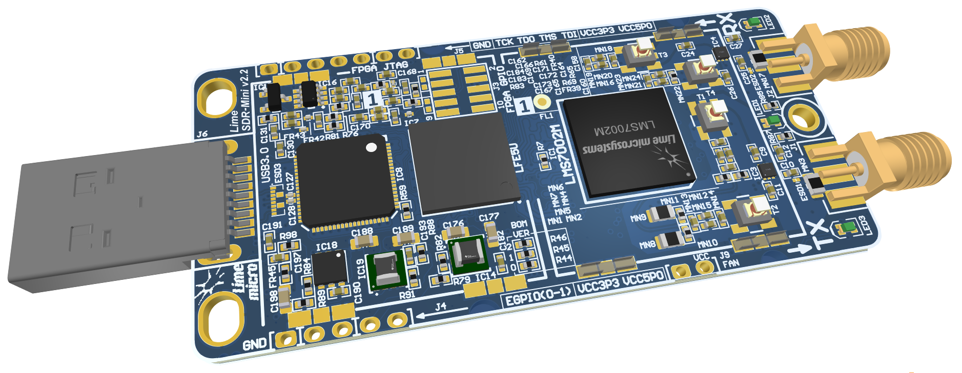
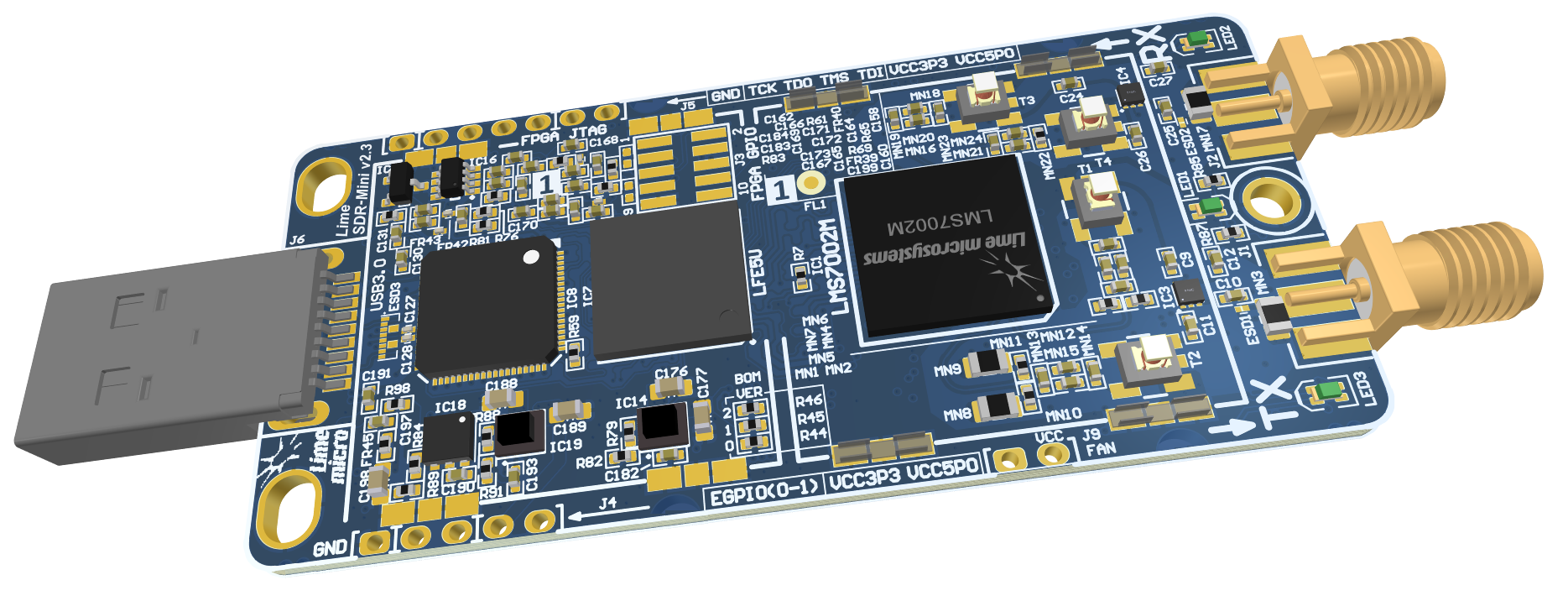
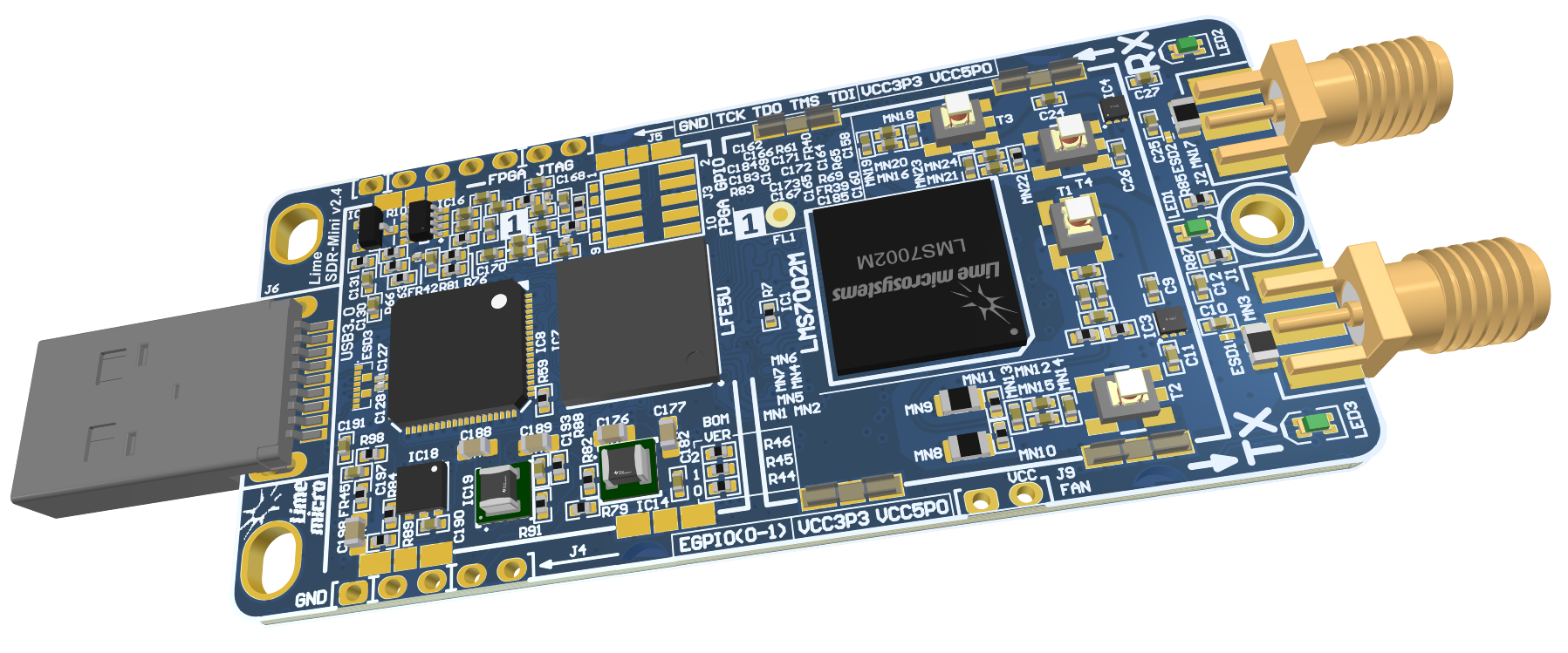
Introduction

LimeSDR Mini is low-cost software defined radio board. LimeSDR Mini development board provides a hardware platform for developing and prototyping high-performance and logic-intensive digital and RF designs based on Lattice Semiconductor’s ECP5 FPGA and Lime Microsystems transceiver.

_images/LimeSDR-Mini_v2.2_3D_top.png

Figure 1: LimeSDR Mini v2.2 board top view

_images/LimeSDR-Mini_v2.2_3D_bot.png

Figure 2: LimeSDR Mini v2.2 board bottom view

LimeSDR Mini board features:

  • RF and BB parameters:

    • Configuration: SISO (1x TX, 1x RX)

    • Frequency range: 10 MHz – 3.5 GHz

    • Bandwidth: 30.72 MHz

    • Sample depth: 12 bit

    • Sample rate: 30.72 MSPS

    • Transmit power: max 10 dBm (depending on frequency)

  • USB 3.0 controller: FTDI FT601

  • FPGA: board is designed for Lattice ECP5 family LFE5U-25F/LFE5U-45F/LFE5U-85F FPGAs in 285-ball csfBGA package. By default board is assembled with LFE5U-45F-MG285 FPGA. Lattice ECP5 LFE5U-45F features:

    • 285-pin csfBGA package (10 x 10 mm, 0.5 mm)

    • 44 K LUTs logic capacity

    • 108 sysMEM Blocks (18 Kb)

    • 1944 Kb Embedded Memory

    • 351 Kb distributed RAM

    • 72x 18x18-bit multipliers

    • 4x PLLs and 4x DLLs

    • 118 IOs

    • FPGA configuration via JTAG

  • RF transceiver: Lime Microsystems LMS7002M

  • EEPROM Memory: 2x 128Kb EEPROMs for LMS MCU firmware and FPGA data (optional)

  • FLASH Memory: 128Mb Flash memory for FPGA configuration

  • Temperature sensor: LM75

  • General user inputs/outputs:

    • 3x Dual colour (RG) LEDs

    • 8x + 2x FPGA GPIO pinheaders (3.3V) (optional)

  • Connections:

    • USB 3.0 (type A) plug

    • Coaxial RF (SMA female) connectors

    • FPGA GPIO headers (unpopulated)

    • FPGA JTAG connector (unpopulated)

    • FAN (5V default or 3.3V) connector

  • Clock system:

    • 40.00MHz on board VCTCXO

    • VCTCXO can be tuned by onboard DAC

    • Reference clock input and output connectors (U.FL)

  • Board size: 69mm x 31.4mm

  • Board power source: USB connector (5V)

For more information on the following topics, refer to the corresponding documents:

Board Overview

The heart of the LimeSDR Mini board is Lattice ECP5 (LFE5U-45F) FPGA. It’s main function is to transfer digital data between the PC through a USB 3.0 connector. The block diagram for LimeSDR Mini board is presented in the Figure 3.

_images/LimeSDR-Mini_v2.2_diagrams_r0_block.png

Figure 3: LimeSDR Mini v2.2 Development Board Block Diagram

This section contains component location description on the board. LimeSDR Mini board picture with highlighted connectors and main components are presented in Figure 4 and Figure 5.

_images/LimeSDR-Mini_v2.2_components_top.png

Figure 4: LimeSDR Mini v2.2 board top connectors and main components

_images/LimeSDR-Mini_v2.2_components_bot.png

Figure 5: LimeSDR Mini v2.2 board bottom connectors and main components

Description of board components is given in the Table 1.

Table 1. Board components

Featured Devices

Board Reference

Type

Description

IC1

RF transceiver

Lime Microsystems LMS7002M

IC7

FPGA

Lattice Semiconductor’s LFE5U (LFE5U-45F)

IC8

USB 3.0 microcontroller

FTDI USB 3.0 to FIFO interface bridge chip FT601

Miscellaneous devices

IC10

IC

Temperature sensor LM75

Configuration, Status and Setup Elements

J5

JTAG chain connector

FPGA programming pin header on the board edge for JTAG cable, 0.1” pitch

LED1, LED2, LED3

Red-green status LEDs

User defined FPGA indication LED.

General User Input/Output

J3

Pin header

8x FPGA GPIOs, 3.3V, 0.05” pitch

J4

Pin header

2x FPGA GPIOs on the board edge, 3.3V, 0.1” pitch

J9

Pin header

5V (3.3V voltage can be chosen by resistors) fan connection pin headers, 0.1” pitch

Memory Devices

IC2

IC

I²C EEPROM Memory 128Kb (16 x 8), connected to RF transceiver I2C bus

IC12

IC

I²C EEPROM Memory 128Kb (16K x 8), connected to FPGA I2C bus

IC15

IC

Quad SPI Flash Memory 128 Mb (16M x 8) connected to FPGA SPI

Communication Ports

J6

USB 3.0 connector

USB 3.0 (type A) plug

Clock Circuitry

XO1

VCTCXO

40.00 MHz Voltage Controlled Temperature Compensated Crystal Oscillator

IC11

IC

10 bit DAC for TCXO (XT4) frequency tuning (default)

IC16

IC

16 bit DAC for TCXO (XT4) frequency tuning (unpopulated)

IC17

IC

Voltage reference (unpopulated)

IC9

IC

Clock buffer

J8

U.FL connector

Reference clock input

J7

U.FL connector

Reference clock output

Power Supply

IC14

IC

Switching regulator LMZ20501 (1.8V rail)

IC19

IC

Switching regulator LMZ20501 (3.3V rail)

IC13

IC

Linear regulator LD39100PUR (1.1V rail)

IC5

IC

Linear regulator LD39100PUR (1.25V rail)

IC6

IC

Linear regulator LD39100PUR (1.4V rail)

IC18

IC

Linear regulator LD39100PUR (2.5V rail)