Board Description
More detailed description of Loamiest Mini board components and interconnections is given in the sections of this chapter.
RF transceiver digital connectivity
The interface and control signals are described below:
Digital Interface Signals: LENS7002 is using data bus LIMNS_DIQ1_D[11:0] and LMS_DIQ2_D[11:0], LMS_EN_IQSEL1 and LMS_EN_IQSEL2, LMS_FCLK1 and LMS_FCLK2, LMS_MCLK1 and LMS_MCLK2 signals to transfer data to/from FPGA. Indexes 1 and 2 indicate transceiver digital data PORT-1 or PORT-2. Any of these ports can be used to transmit or receive data. By default PORT-1 is selected as transmit port and PORT-2 is selected as receiver port. The FCLK# is input clock and MCLK# is output clock for LMS7002M transceiver. TXNRX signals sets ports directions. For LMS7002M interface timing details refer to LMS7002M transceiver datasheet page 12-13.
LMS Control Signals: these signals are used for optional functionality: * LMS_RXEN, LMS_TXEN – receiver and transmitter enable/disable signals connected to FPGA Bank 8 (VDIO_LMS_FPGA; 2.5V). * LMS_RESET – LMS7002M reset connected to FPGA Bank 3 (VDIO_LMS_FPGA; 2.5V).
SPI Interface: LMS7002M transceiver is configured via 4-wire SPI interface; FPGA_SPI_SCLK, FPGA_SPI_MOSI, FPGA_SPI_MISO, FPGA_SPI_LMS_SS. The SPI interface controlled from FPGA Bank 3 (VDIO_LMS_FPGA; 2.5V).
LMS I2C Interface: can be used for LMS EEPROM content modifying or for debug purposes. The signals LMS_I2C_SCL, LMS_I2C_DATA connected to EEPROM.
Chip pin (IC1) |
Chip reference (IC1) |
Schematic signal name |
FPGA pin |
FPGA I/O standard |
FPGA I/O standard |
|---|---|---|---|---|---|
E5 |
xoscin_tx |
TxPLL_CLK |
Connected to 40.00 MHz clock |
||
AB34 |
MCLK1 |
LMS_MCLK1 |
H4 |
2.5V/3.3V |
|
AA33 |
FCLK1 |
LMS_FCLK1 |
H3 |
2.5V/3.3V |
|
V32 |
TXNRX1 |
LMS_TXNRX1 |
F1 |
2.5V/3.3V |
|
U29 |
TXEN |
LMS_TXEN |
B7 |
2.5V/3.3V |
|
1Y32 |
ENABLE_IQSEL1 |
LMS_EN_IQSEL1 |
F3 |
2.5V/3.3V |
|
AG31 |
DIQ1_D0 |
LMS_DIQ1_D0 |
J2 |
2.5V/3.3V |
|
AF30 |
DIQ1_D1 |
LMS_DIQ1_D1 |
L1 |
2.5V/3.3V |
|
AF34 |
DIQ1_D2 |
LMS_DIQ1_D2 |
K1 |
2.5V/3.3V |
|
AE31 |
DIQ1_D3 |
LMS_DIQ1_D3 |
K4 |
2.5V/3.3V |
|
AD30 |
DIQ1_D4 |
LMS_DIQ1_D4 |
G3 |
2.5V/3.3V |
|
AC29 |
DIQ1_D5 |
LMS_DIQ1_D5 |
F4 |
2.5V/3.3V |
|
AE33 |
DIQ1_D6 |
LMS_DIQ1_D6 |
J1 |
2.5V/3.3V |
|
AD32 |
DIQ1_D7 |
LMS_DIQ1_D7 |
H1 |
2.5V/3.3V |
|
AC31 |
DIQ1_D8 |
LMS_DIQ1_D8 |
G4 |
2.5V/3.3V |
|
AC33 |
DIQ1_D9 |
LMS_DIQ1_D9 |
F2 |
2.5V/3.3V |
|
AB30 |
DIQ1_D10 |
LMS_DIQ1_D10 |
G1 |
2.5V/3.3V |
|
AB32 |
DIQ1_D11 |
LMS_DIQ1_D11 |
H2 |
2.5V/3.3V |
|
AM24 |
xoscin_rx |
RxPLL_CLK |
Connected to 40.00 MHz clock |
||
P34 |
MCLK2 |
LMS_MCLK2 |
D2 |
2.5V/3.3V |
|
R29 |
FCLK2 |
LMS_FCLK2 |
D1 |
2.5V/3.3V |
|
U31 |
TXNRX2 |
LMS_TXNRX2 |
B6 |
2.5V/3.3V |
|
V34 |
RXEN |
LMS_RXEN |
D6 |
2.5V/3.3V |
|
R33 |
ENABLE_IQSEL2 |
LMS_EN_IQSEL2 |
C4 |
2.5V/3.3V |
|
H30 |
DIQ2_D0 |
LMS_DIQ2_D0 |
A3 |
2.5V/3.3V |
|
J31 |
DIQ2_D1 |
LMS_DIQ2_D1 |
C2 |
2.5V/3.3V |
|
K30 |
DIQ2_D2 |
LMS_DIQ2_D2 |
A2 |
2.5V/3.3V |
|
K32 |
DIQ2_D3 |
LMS_DIQ2_D3 |
B4 |
2.5V/3.3V |
|
L31 |
DIQ2_D4 |
LMS_DIQ2_D4 |
C3 |
2.5V/3.3V |
|
K34 |
DIQ2_D5 |
LMS_DIQ2_D5 |
B2 |
2.5V/3.3V |
|
M30 |
DIQ2_D6 |
LMS_DIQ2_D6 |
D3 |
2.5V/3.3V |
|
M32 |
DIQ2_D7 |
LMS_DIQ2_D7 |
B1 |
2.5V/3.3V |
|
N31 |
DIQ2_D8 |
LMS_DIQ2_D8 |
A4 |
2.5V/3.3V |
|
N33 |
DIQ2_D9 |
LMS_DIQ2_D9 |
C1 |
2.5V/3.3V |
|
P30 |
DIQ2_D10 |
LMS_DIQ2_D10 |
C7 |
2.5V/3.3V |
|
P32 |
DIQ2_D11 |
LMS_DIQ2_D11 |
A6 |
2.5V/3.3V |
|
U33 |
CORE_LDO_EN |
LMS_CORE_LDO_EN |
C6 |
2.5V/3.3V |
|
E27 |
RESET |
LMS_RESET |
A7 |
2.5V/3.3V |
|
D28 |
SEN |
FPGA_SPI_LMS_SS |
N3 |
2.5V/3.3V |
SPI interface |
C29 |
SCLK |
FPGA_SPI_SCLK |
M3 |
2.5V/3.3V |
SPI interface |
F30 |
SDIO |
FPGA_SPI_MOSI |
L3 |
2.5V/3.3V |
SPI interface |
F28 |
SDO |
FPGA_SPI_MISO |
K3 |
2.5V/3.3V |
SPI interface |
D26 |
SDA |
LMS_I2C_SDA |
Connected to EEPROM |
||
C27 |
SCL |
LMS_I2C_SCL |
Connected to EEPROM |
RF path and control signals
LimeSDR Mini RF path contains matching networks, RF switches, loopback variable attenuator and 2 SMA connectors (J1 - TX and J2 - RX) as shown in Figure 1.
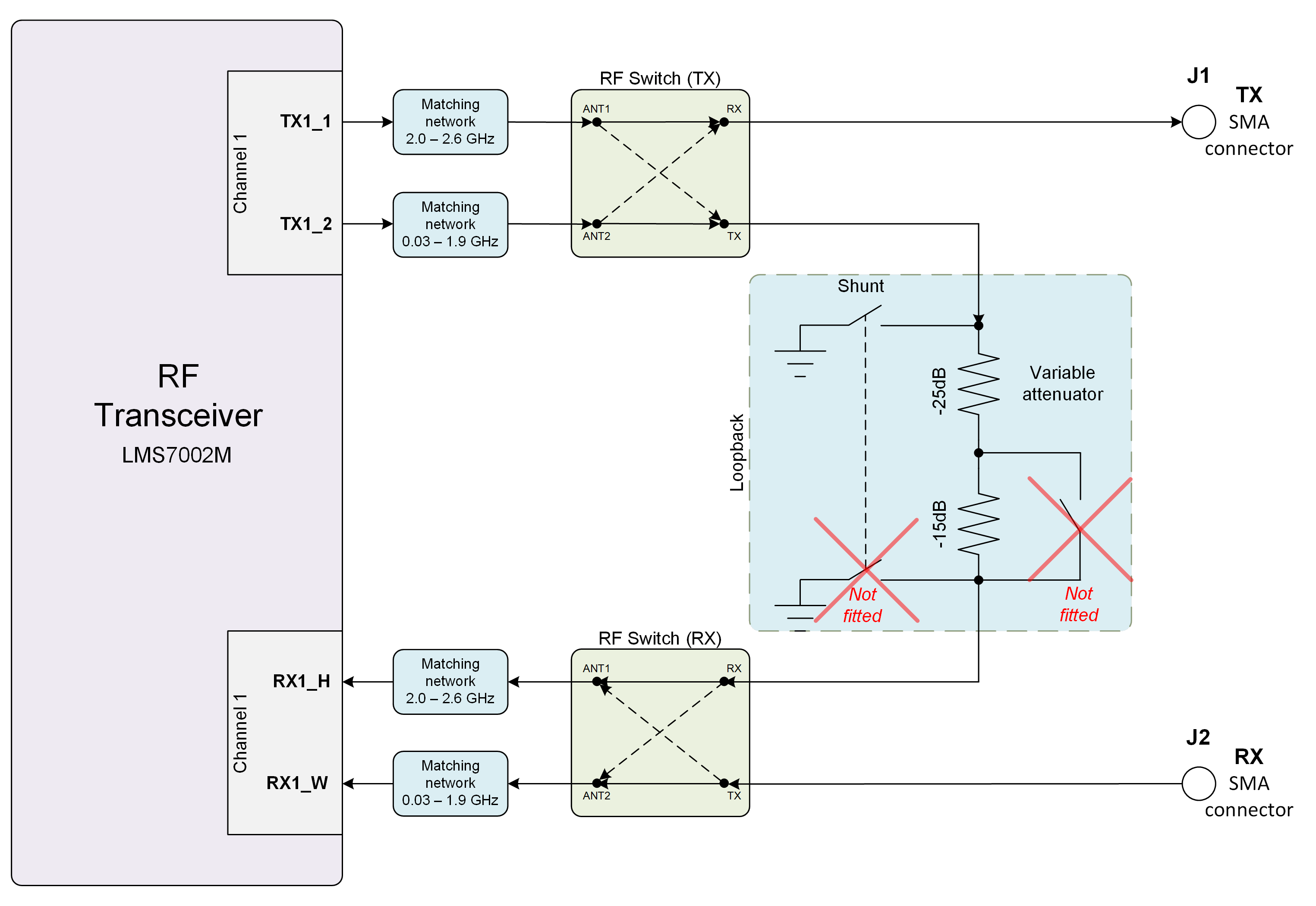
Figure 1: LimeSDR Mini v2.2 RF diagram
RF transceiver TX and RX ports has its dedicated matching network which together determines the working frequency range. More detailed information about RF transceiver ports and matching network frequency ranges is listed in the Table 2.
RF transceiver port |
Frequency range |
|---|---|
TX1_1 |
2 GHz - 2.6 GHz |
TX1_2 |
30 MHz - 1.9 GHz |
RX1_H |
2 GHz - 2.6 GHz |
RX1_W |
700 MHz - 900 MHz |
RF path control signals are described in the Table 3.
Component |
Schematic signal name |
I/O standard |
FPGA pin |
Description |
|---|---|---|---|---|
RFSW_TX (SKY13411-374LF – IC3) |
RFSW_TX_V1 |
3.3V |
B10 |
V1 – high V2- low TX1_1 to TX and TX1_2 to ATT, V1 – low V2 – high TX1_1 to ATT and TX1_2 to TX |
RFSW_TX_V2 |
3.3V |
C9 |
||
RFSW_RX (SKY13411-374LF – IC3) |
RFSW_RX_V1 |
3.3V |
C11 |
V1 – high V2- low RX_H to RX and RX1_W to ATT, V1 – low V2 – high RX1_H to ATT and RX1_W to RX |
RFSW_RX_V2 |
3.3V |
B11 |
||
Variable attenuator |
TX_LB_AT |
3.3V |
C8 |
High - -40dB, low - -25dB |
TX_LB_SH |
3.3V |
B8 |
Attenuator shunting. |
Notes on RF loopback
LimeSDR Mini v2.X encountered a change of shunt transistor VT3 in the RF feedback attenuator chain due to the original part becoming EOL. The original part BFT92,215 had a small output capacitance of around 1.2 pF, whereas the new RF transistor ZVN4525E6TA has a larger output capacitance of 11 pF. An extract of the schematic is presented in Figure 2.
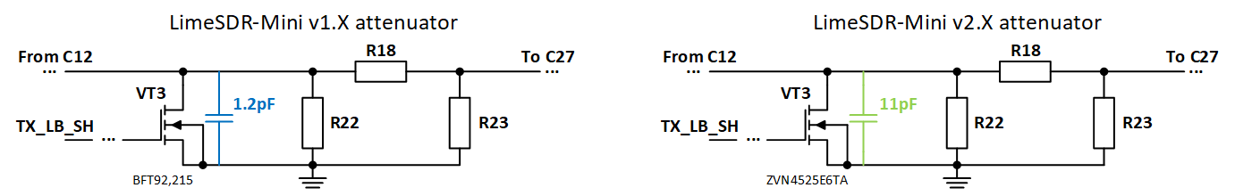
Figure 2: LimeSDR Mini RF loopback attenuator implementation on v1.x and v2.x boards
The increased shunt capacitance affects a frequency response of the attenuator as shown in Figure 3. The attenuation is −46 dB at 1 GHz and −52 dB at 2.1 GHz for the new LimeSDR-Mini v2.X board. The frequency response shown in Figure 3 can be used as a reference RF loopback attenuation in the supported frequency range.
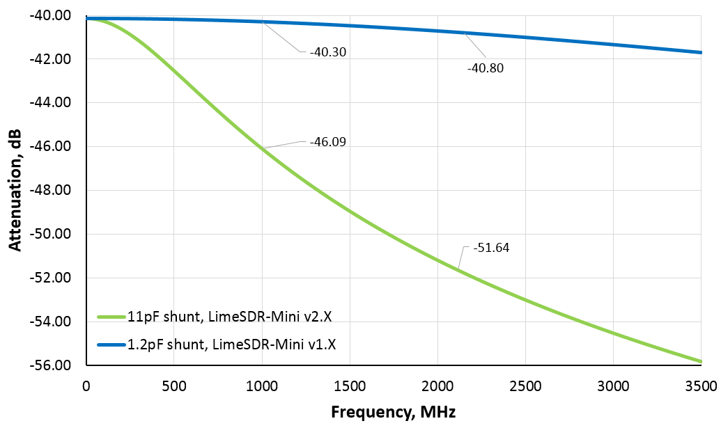
Figure 3: LimeSDR Mini v2.2 RF loopback frequency response
USB 3.0 controller
Software controls LimeSDR Mini board via the USB 3.0 controller (FTDI USB 3.0 to FIFO interface bridge chip FT601 [link]). The controller signals description showed below:
FT_D[31:0] – FTDI 32-bit data interface is connected to FPGA.
FT_TXEn, FT_RXFn, FT_SIWUn, FT_WRn, FT_RDn, FT_OEn, FT_BE[3:0] – FTDI interface control signals.
FT_CLK – FTDI interface clock. Clock from FTDI is fed to FPGA.
More information about USB 3.0 controller (FTDI) pins, schematic signal names, FPGA interconnections and I/O standards is given in Table 4.
Chip pin (IC6) |
Chip reference (IC6) |
Schematic signal name |
FPGA pin |
I/O standard |
Comment |
|---|---|---|---|---|---|
40 |
DATA_0 |
FT_D0 |
A13 |
3.3V |
|
41 |
DATA_1 |
FT_D1 |
B12 |
3.3V |
|
42 |
DATA_2 |
FT_D2 |
B15 |
3.3V |
|
43 |
DATA_3 |
FT_D3 |
C12 |
3.3V |
|
44 |
DATA_4 |
FT_D4 |
A16 |
3.3V |
|
45 |
DATA_5 |
FT_D5 |
A12 |
3.3V |
|
46 |
DATA_6 |
FT_D6 |
D18 |
3.3V |
|
47 |
DATA_7 |
FT_D7 |
B17 |
3.3V |
|
50 |
DATA_8 |
FT_D8 |
F15 |
3.3V |
|
51 |
DATA_9 |
FT_D9 |
D16 |
3.3V |
|
52 |
DATA_10 |
FT_D10 |
D15 |
3.3V |
|
53 |
DATA_11 |
FT_D11 |
C13 |
3.3V |
|
54 |
DATA_12 |
FT_D12 |
H18 |
3.3V |
|
55 |
DATA_13 |
FT_D13 |
B13 |
3.3V |
|
56 |
DATA_14 |
FT_D14 |
J18 |
3.3V |
|
57 |
DATA_15 |
FT_D15 |
A15 |
3.3V |
|
60 |
DATA_16 |
FT_D16 |
B18 |
3.3V |
|
61 |
DATA_17 |
FT_D17 |
C18 |
3.3V |
|
62 |
DATA_18 |
FT_D18 |
A17 |
3.3V |
|
63 |
DATA_19 |
FT_D19 |
K18 |
3.3V |
|
64 |
DATA_20 |
FT_D20 |
C15 |
3.3V |
|
65 |
DATA_21 |
FT_D21 |
L18 |
3.3V |
|
66 |
DATA_22 |
FT_D22 |
F18 |
3.3V |
|
67 |
DATA_23 |
FT_D23 |
C16 |
3.3V |
|
69 |
DATA_24 |
FT_D24 |
G16 |
3.3V |
|
70 |
DATA_25 |
FT_D25 |
D13 |
3.3V |
|
71 |
DATA_26 |
FT_D26 |
G18 |
3.3V |
|
72 |
DATA_27 |
FT_D27 |
F16 |
3.3V |
|
73 |
DATA_28 |
FT_D28 |
C17 |
3.3V |
|
74 |
DATA_29 |
FT_D29 |
F17 |
3.3V |
|
75 |
DATA_30 |
FT_D30 |
K15 |
3.3V |
|
76 |
DATA_31 |
FT_D31 |
K17 |
3.3V |
|
58 |
CLK |
FT_CLK |
D17 |
3.3V |
|
4 |
BE_0 |
FT_BE0 |
L15 |
3.3V |
|
5 |
BE_1 |
FT_BE1 |
J17 |
3.3V |
|
6 |
BE_2 |
FT_BE2 |
K16 |
3.3V |
|
7 |
BE_3 |
FT_BE3 |
H17 |
3.3V |
|
8 |
TXE_N |
FT_TXEn |
M16 |
3.3V |
|
9 |
RXF_N |
FT_RXFn |
H16 |
3.3V |
|
10 |
SIWU_N |
FT_SIWUn |
3.3V |
10k pull up |
|
11 |
WR_N |
FT_WRn |
J16 |
3.3V |
|
12 |
RD_N |
FT_RDn |
H15 |
3.3V |
|
13 |
OE_N |
FT_OEn |
L16 |
3.3V |
|
15 |
RESET_N |
FT_RESETn |
M17 |
3.3V |
|
16 |
WAKEP_N |
FT_WAKEUPn |
G15 |
3.3V |
Indication LEDs
LimeSDR Mini board comes with three dual colour (red and green (RG)) indication LEDs. These LEDs are soldered on the top of the board near RF connectors.
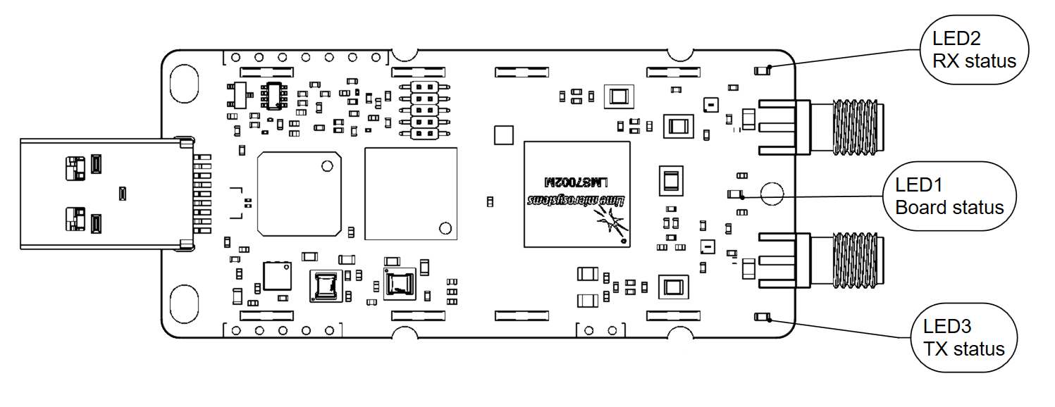
Figure 4: LimeSDR Mini indication LEDs (top and bottom)
LEDs are connected to FPGA and their function may be programmed according to the user requirements. Default function of LEDs and related information is listed in Table 5.
Board reference |
Schematic name |
Board label |
FPGA pin |
Comment |
|---|---|---|---|---|
LED1 |
FPGA_LED1_R |
LED1 |
V17 |
Board status: Blinking green = LMK_CLK clock is running; Red = USB control port is active. |
FPGA_LED1_G |
R16 |
|||
LED2 |
FPGA_LED2_R |
LED2 |
R18 (FPGA_GPIO5) |
RX status: Green = DIQ data receive enabled; Off = DIQ data receive disabled. Shared with FPGA_GPIO4 and FPGA_GPIO5. |
FPGA_LED2_G |
M18 (FPGA_GPIO4) |
|||
LED3 |
FPGA_LED3_R |
LED3 |
R17 (FPGA_GPIO7) |
TX status: Red = transmitting DIQ data; Off = no activity. Shared with FPGA_GPIO6 and FPGA_GPIO7. |
FPGA_LED3_G |
T17 (FPGA_GPIO6) |
Low speed interfaces
To control on board infrastructure various low speed interfaces are implemented.
LMS7002M RF transceiver and VCTCXO DAC are controlled via SPI interface. Deatils of this interface are given in Table 6.
Schematic signal name |
FPGA pin |
I/O standard |
Comment |
|---|---|---|---|
FPGA_SPI_SCLK |
M3 |
2.5V /3.3V |
Serial Clock (FPGA output) |
FPGA_SPI_MOSI |
L3 |
2.5V /3.3V |
Data (FPGA output) |
FPGA_SPI_MISO |
K3 |
2.5V /3.3V |
Data (FPGA input) |
FPGA_SPI_LMS_SS |
N3 |
2.5V /3.3V |
IC1 (LMS7002) SPI slave select (FPGA output) |
FPGA_SPI_DAC_SS |
L4 |
2.5V /3.3V |
IC11 SPI slave select (FPGA output) |
FPGA configuration flash memory is connected via separate SPI bus, more information is given in Table 7.
Schematic signal name |
FPGA pin |
I/O standard |
Comment |
|---|---|---|---|
FPGA_CFG_SPI_SCLK |
U16 |
3.3V |
Serial Clock (FPGA output) |
FPGA_CFG_SPI_MOSI |
U18 |
3.3V |
|
FPGA_CFG_SPI_MISO |
T18 |
3.3V |
|
FPGA_CFG_SPI_SS |
U17 |
3.3V |
IC15 SPI slave select (FPGA output) |
There is temperature sensor and EEPROM memory connected to the FPGA via I2C bus. Deatils of this interface are given in Table 8.
I2C slave device |
Slave device |
I2C address |
I/O standard |
Comment |
|---|---|---|---|---|
IC10 |
Temperature sensor |
1 0 0 1 0 0 0 RW |
3.3V |
LM75 |
IC12 |
EEPROM |
1 0 1 0 0 0 0 RW |
3.3V |
M24128 |
GPIO connectors
Eight GPIOs from FPGA are connected to 10 pin 0.05” header. Additional 2 pins are dedicated for power. FPGA_GPIO[7:4] are shared with TX and RX LEDs. Remove solder from solder bridges to disconnect LEDs from GPIOs lines if required. More information about GPIO connector J3 is given in Table 9.
Connector pin |
Schematic signal name |
FPGA pin |
I/O standard |
Comment |
|---|---|---|---|---|
1 |
FPGA_GPIO0 |
N15 |
3.3V |
|
2 |
FPGA_GPIO1 |
N18 |
3.3V |
|
3 |
FPGA_GPIO2 |
N16 |
3.3V |
|
4 |
FPGA_GPIO3 |
N17 |
3.3V |
|
5 |
FPGA_GPIO4 |
M18 |
3.3V |
Shared with FPGA_LED2_G |
6 |
FPGA_GPIO5 |
R18 |
3.3V |
Shared with FPGA_LED2_R |
7 |
FPGA_GPIO6 |
T17 |
3.3V |
Shared with FPGA_LED3_G |
8 |
FPGA_GPIO7 |
R17 |
3.3V |
Shared with FPGA_LED3_R |
9 |
GND |
Ground pin |
||
10 |
Selectable power net (3.3V or 5V). Default 3.3V |
Another 2 GPIOs are connected to 5 pin header on the board edge. More information about FPGA_EGPIO connector J7 is given in Table 10.
Connector pin |
Schematic signal name |
FPGA pin |
I/O standard |
Comment |
|---|---|---|---|---|
1 |
GND |
Ground pin |
||
2 |
FPGA_EGPIO0 |
A10 |
3.3V |
|
3 |
FPGA_EGPIO1 |
A8 |
3.3V |
|
4 |
VCC3P3 |
3.3V |
Power net (3.3V) |
|
5 |
VCC5P0 |
5.0V |
Power net (5.0V) |
JTAG interface
To debug FPGA design, flash bitstream to FPGA and/or Flash memory JTAG is used. It is located on the PCB top side (see Figure 4: LimeSDR Mini v2.2 board top connectors and main components) and attaches to the programmer using 7-pin, 0.1” spaced JTAG connector J5. JTAG connector pins, schematic signal names, FPGA interconnections and I/O standards are listed in Table 11.
6
FPGA_GPIO5
R18
3.3V
Shared with FPGA_LED2_R
7
FPGA_GPIO6
T17
3.3V
Shared with FPGA_LED3_G
8
FPGA_GPIO7
R17
3.3V
Shared with FPGA_LED3_R
9
GND
Ground pin
10
Selectable power net (3.3V or 5V). Default 3.3V
Another 2 GPIOs are connected to 5 pin header on the board edge. More information about FPGA_EGPIO connector J7 is given in Table 10.
Connector pin |
Schematic signal name |
FPGA pin |
I/O standard |
Comment |
|---|---|---|---|---|
1 |
GND |
Ground |
||
2 |
TCK |
U13 |
3.3V |
Test Clock |
3 |
TDO |
V14 |
3.3V |
Test Data Out |
4 |
TMS |
V13 |
3.3V |
Test Mode Select |
5 |
TDI |
T13 |
3.3V |
Test Data In |
6 |
VCC3P3 |
Power (3.3V) |
||
7 |
VCC5P0 |
Power (5.0V) |
More information about JTAG programming can be found in section 3.
Board temperature control
LimeSDR Mini has integrated temperature sensor which controls FAN to keep board in operating temperature range. FAN must be connected to J9 (0.1” pitch) connector. FAN control voltage y default is 5V, but it can be changed to 3.3V by resistors.
Fan will be turned on if board will heat up to 55°C and FAN will be turned off if board will cool down to 45°C.
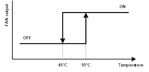
Figure 5: FAN control temperature hysteresis
Clock distribution
LimeSDR Mini board clock distribution block diagram is presented in Figure 6. LimeSDR Mini board has onboard 40.00 MHz VCTCXO that is reference clock for RF transceiver and FPGA PLLs.
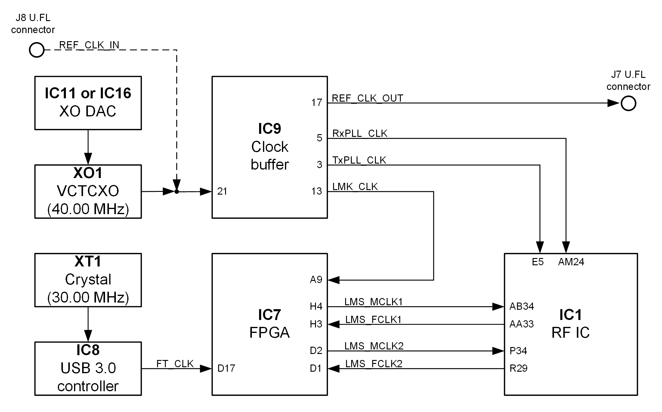
Figure 6: LimeSDR Mini v2.2 board clock distribution block diagram
Rakon E7355LF 40 MHz voltage controlled temperature compensated crystal oscillator (VCTCXO) is main board clock source. VCTCXO frequency can be tuned by using DAC (IC11 10 bit or IC16 16 bit (unpopulated)). Main VCTCXO parameters are listed in Table 12.
Frequency parameter |
Value |
|---|---|
Calibration (25°C ± 1°C) |
± 1 ppm max |
Stability (-40 to 85 °C) |
± 0.5 max |
Long term stability (1 year, 10 years) |
± 2 ppm max, ± 4 ppm max |
Control voltage range |
0.5V .. 2.5V |
Frequency tuning |
± 7 ppm min, ± 15 ppm max |
Slope |
+9 ppm/V |
VCTCXO clock is connected to clock buffer IC9. Buffered VCTCXO clock is connected to RF transceiver, FPGA. Buffered VCTCXO clock is also connected to connector J7 (REF_CLK_OUT) and can be fed to external hardware for synchronisation. VCTCXO clock can be disconnected from clock buffer input (remove R63 and solder R66) and external reference clock can be supplied from connector J8 (REF_CLK_IN) instead of VCTCXO (40 MHz). Main board clock lines and other related information are listed in Table 13.
Source |
Schematic signal name |
I/O standard |
FPGA pin |
Description |
|---|---|---|---|---|
External |
REF_CLK_IN |
2.5V/3.3V |
External reference clock input |
|
Clock buffer (IC9) |
REF_CLK_OUT |
3.3V |
Reference clock output |
|
Clock buffer (IC9) |
LMK_CLK |
3.3V |
A9 |
Reference clock connected to FPGA |
RF transceiver (IC1) |
RxPLL_CLK |
1.8V |
Reference clock input |
|
TxPLL_CLK |
1.8V |
Reference clock input |
||
LMS_MCLK1 |
2.5V/3.3V |
H4 |
||
LMS_FCLK1 |
2.5V/3.3V |
H3 |
||
LMS_MCLK2 |
2.5V/3.3V |
D2 |
||
LMS_FCLK2 |
2.5V/3.3V |
D1 |
||
USB 3.0 controller (IC8) |
FT_CLK |
3.3V |
D17 |
Clock output (100 MHz) from USB controller |
Power distribution
LimeSDR Mini board is powered from USB port (5V). LimeSDR Mini board power delivery network consists of different power rails with different voltages, filters, power sequences. LimeSDR Mini board power distribution block diagram is presented in Figure 7.
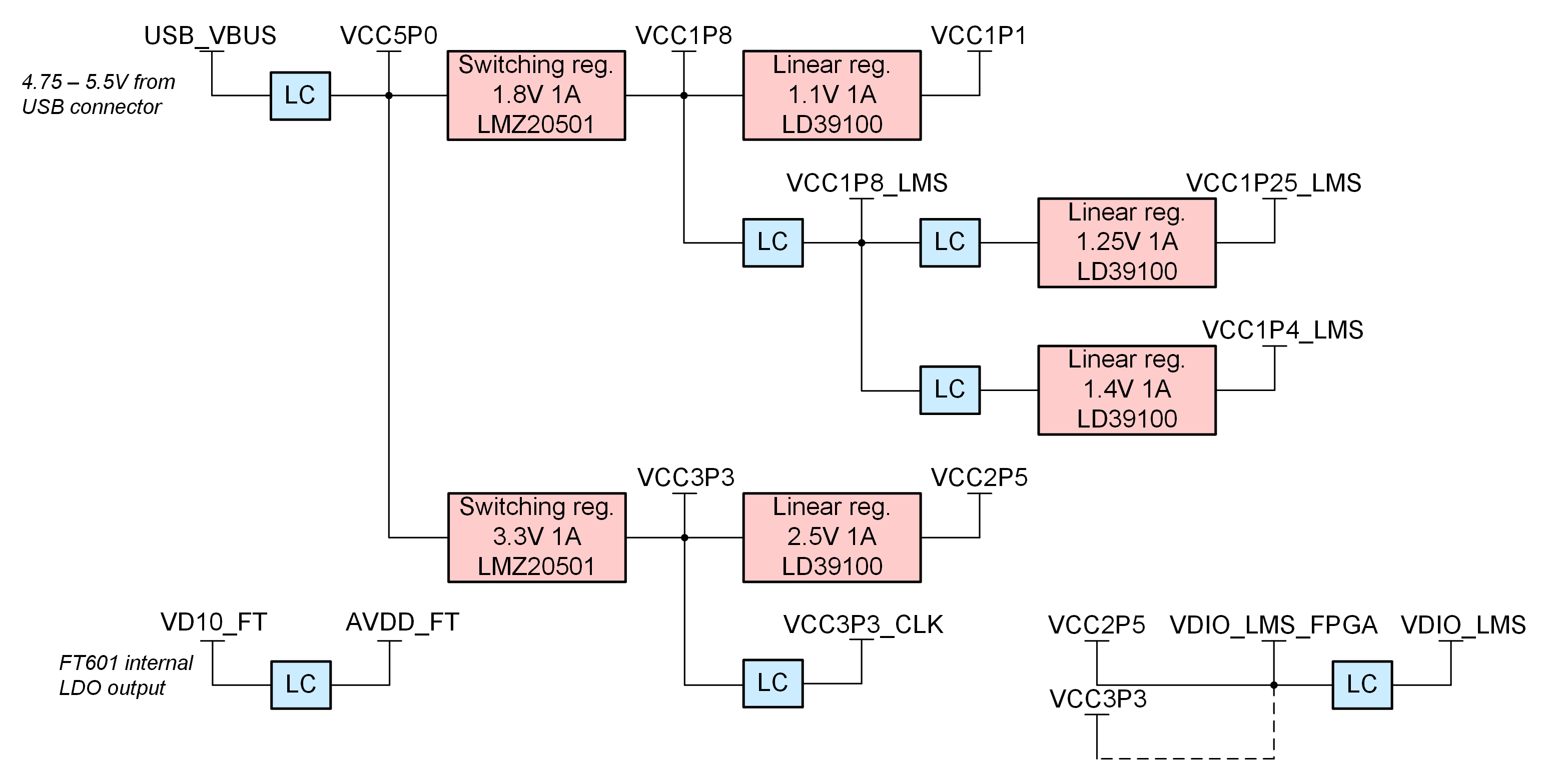
Figure 7: LimeSDR Mini v2.2 board power distribution block diagram
Fan mounting
LimeSDR Mini v2.2 board features three holes which may be used to secure the board into the case or fan mounting for instance as shown in Figure 8. Two holes are placed at the sides of USB connector and one more hole is between SMA connectors.
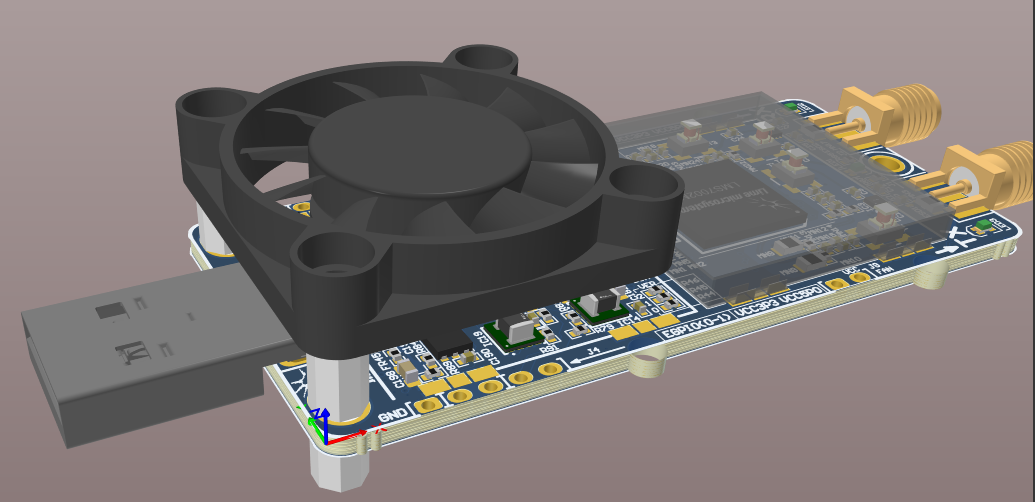
Figure 8: LimeSDR Mini v2.2 fan mounting
Warning
You have to be careful when using mounting holes not to damage R72 resistor and C186 capacitor while there is no much clearence as you may see in Figure 9.
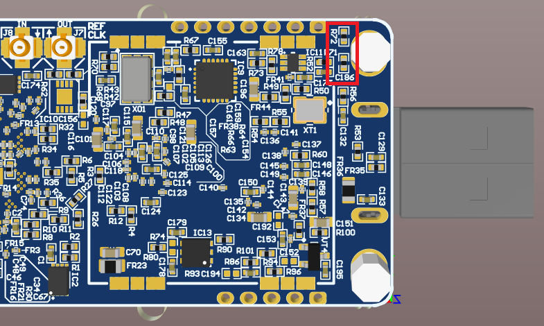
Figure 10: LimeSDR Mini v2.2 mounting hole clearence
Recommended fan mounting solution is shown in Figure 8.
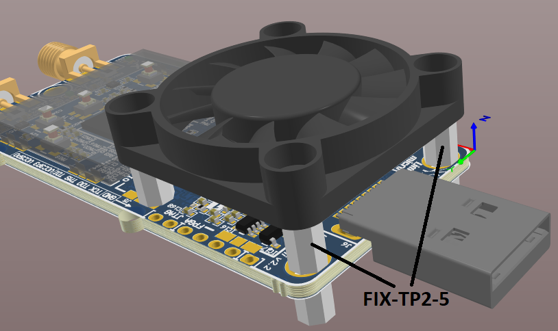
Figure 11: FIX-TP2-5 fan mounting components
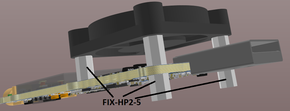
Figure 12: FIX-HP2-5 fan mounting components
Use two FIX-TP2-5 stands with internal and external thread (4mm width, M2 thread) as a spacers to mount the fan on top of LimeSDR Mini v2.2. Put FIX-TP2-5 stands from the top through LimeSDR Mini v2.2 slot mounting holes around USB connector as shown in Figure 11. Secure the stands to the fan using two M2 thread screws (ex. P/N 1219480, Phillips head screw, M2x10). Secure two FIX-TP2-5 stands using two FIX-HP2-5 spacers as nuts from the bottom of the PCB as shown in Figure 12. This is enough to hold the fan but one may use additional FIX-HP2-5 (4mm width, M2 thread) stand with internal thread as an additional fan rest point which rests on PCB over unmounted J3 connector as shown in Figures 11 and 12. Secure FIX-HP2-5 spacer to the fan using the same screw (P/N 1219480).
Total required mechanical components per LimeSDR Mini v2.2:
2x FIX-TP2-5 stands with internal and external M2 thread;
3x FIX-HP2-5 stands with internal M2 threads;
3x 1219480 screws; M2x10 10mm length;
1x 4127/MF30060V1-1000U-A99 30mm fan.