JTAG Programming
This section describes how to program the Lattice LFE5U FPGA used on the LimeSDR Mini v2 board using JTAG interface, FT2232H Mini Module and Lattice software.
Used software
List of used software is given in Table 1.
Tool |
Version |
Comment |
|---|---|---|
3.12 SP1 |
Standalone programing software for 64-bit Windows OS. Also available for Linux OS. |
|
Production Build 3.12.0.240.2 |
FPGA design and programming software |
|
Build 3.12.1.454.2 |
Update for Lattice Diamond (Optional) |
|
1.1 |
Mico32 CPU integration tool (Optional) |
Connecting LimeSDR Mini v2 board to FT2232H Mini Module
FTDI FT2232H Mini Module is available for approximately $20 from distributors like Digi-Key and Mouser, and it can be used directly as a programming adapter for Lattice devices (and others) by following the setup described below. JTAG is a 4-wire protocol defined by the IEEE (Std 1149.1-2013). The signals that comprise the Test Access Port (TAP) are TCK, TMS, TDI, and TDO. The FT2232H is a two port bridge device and either port can be used for JTAG. Our configuration makes use of bus/port A (0).
FT2232H Mini Module preparation:
Connect CN3-1 to CN3-3, which connects USB VBUS to VCC (voltage regulator input). This can be done using jumper.
Connect LimeSDR Mini v2 to FT2232H Mini module as specified in Table 2 (see Figure 1 for graphical representation).
LimeSDR Mini v2 |
FT2232H Mini module |
|---|---|
J5-1 (GND) |
CN2-2 (GND) |
J5-2 (FPGA_JTAG_TCK) |
CN2-7 (AD0) |
J5-3 (FPGA_JTAG_TDO) |
CN2-9 (AD2) |
J5-4 (FPGA_JTAG_TMS) |
CN2-12 (AD3) |
J5-5 (FPGA_JTAG_TDI) |
CN2-10 (AD1) |
J5-6 (VCC3P3) |
CN2-11 (VIO) |
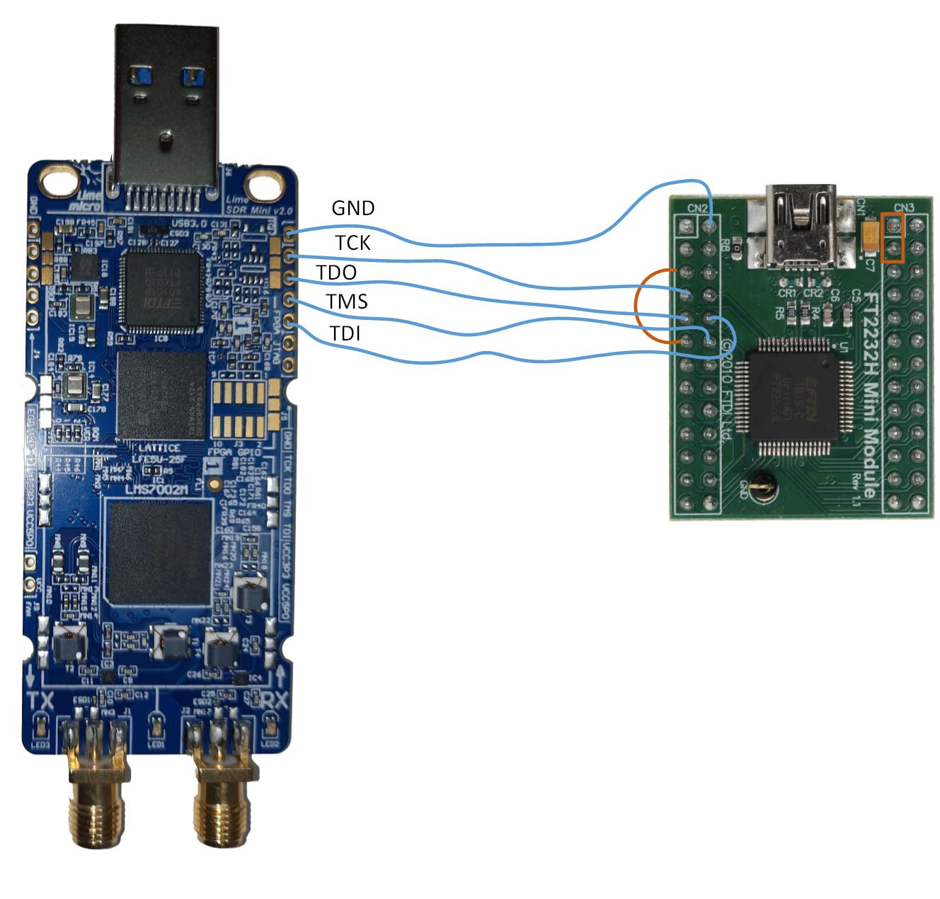
Figure 1: LimeSDR Mini v2 board and FT2232H Mini module connections
FPGA programming using Lattice Diamond Programmer software
Creating a new project
Connect LimesdSDR Mini v2 board to FTDI FT2232H Mini Module as described in paragraph above and connect them to PC via USB ports. Launch software “Lattice Diamond Programmer”. Cable HW-USBN-2B (FTDI) and port FTUSB-0 must be selected, as shown in Figure 2.
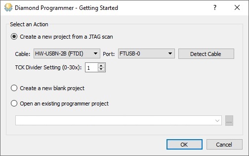
Figure 2: Cable and port selection
Select an action “Create a new project from JTAG scan” and press “OK” button. Device database loading and JTAG scanning procedures will start, as shown in Figure 3.
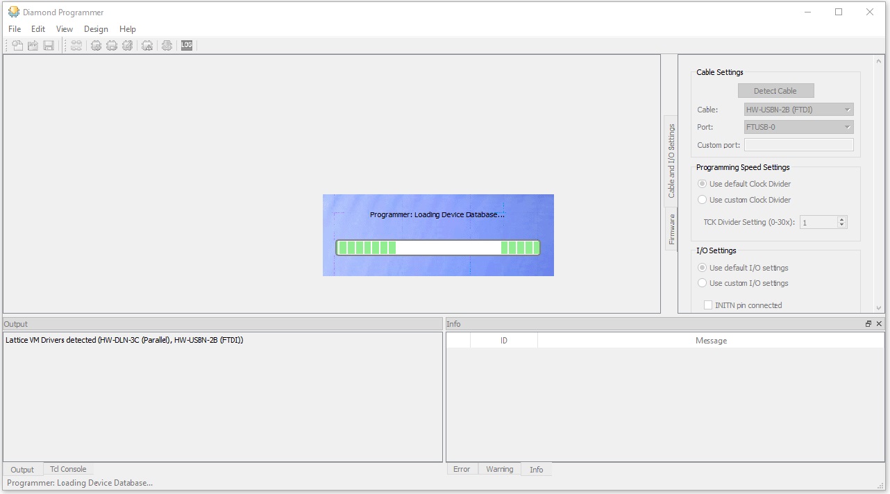
Figure 3: Device database loading and JTAG scanning procedure
After successful JTAG chain scan ECP5U family FPGA device will be detected (in this case LFE5U-45F), as shown in Figure 4.
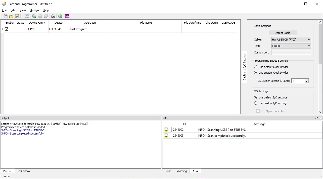
Figure 4: Detected FPGA device
RAM programming
In context menu press “Edit -> Device properties” and set device operation parameters as shown in Figure 5. Also load appropriate programming file (gateware, bitstream) and then press “OK”.
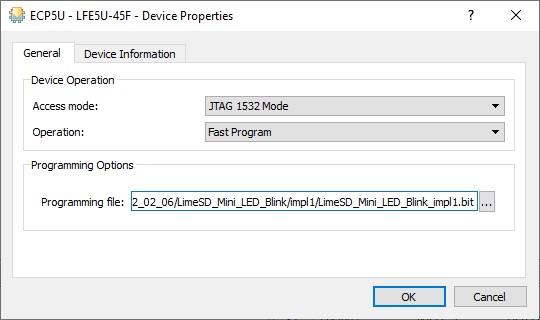
Figure 5: Device operation parameters and programming file
The main program window should look as shown in Figure 6.
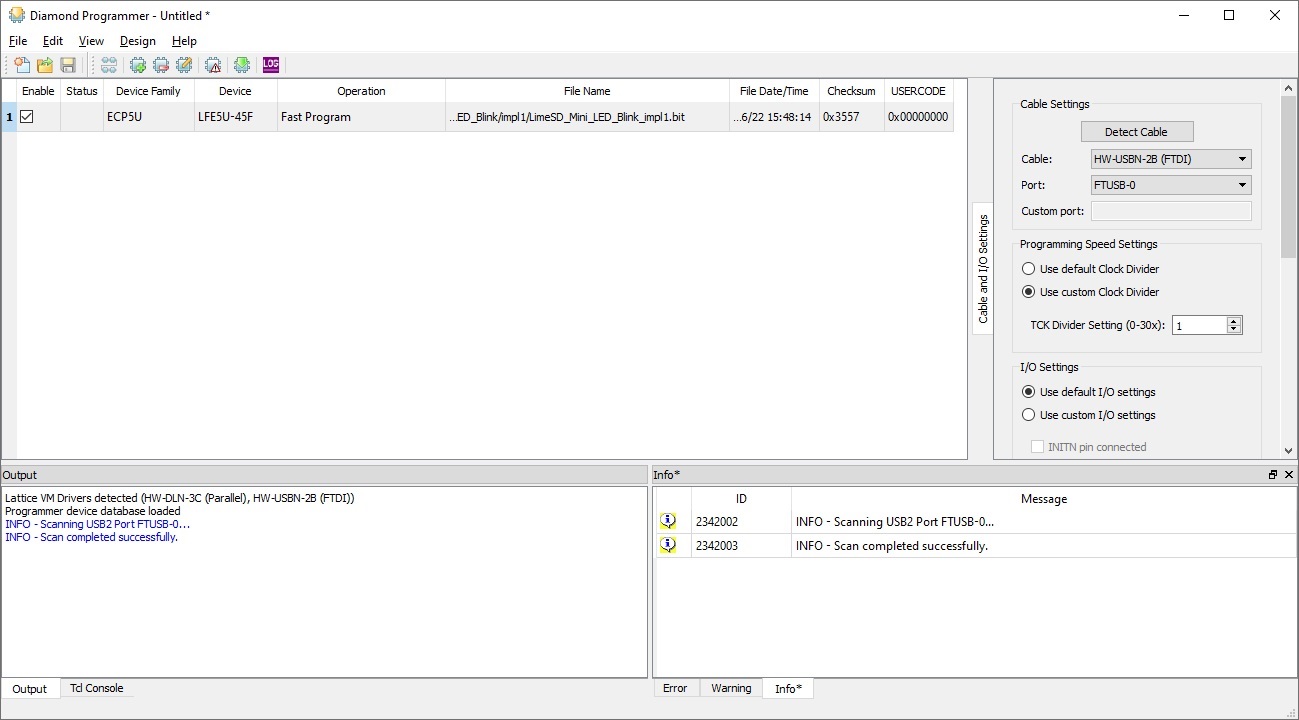
Figure 6: Main program window
In context menu press “Design -> Program” and RAM programming procedure will start, as shown in Figure 7.
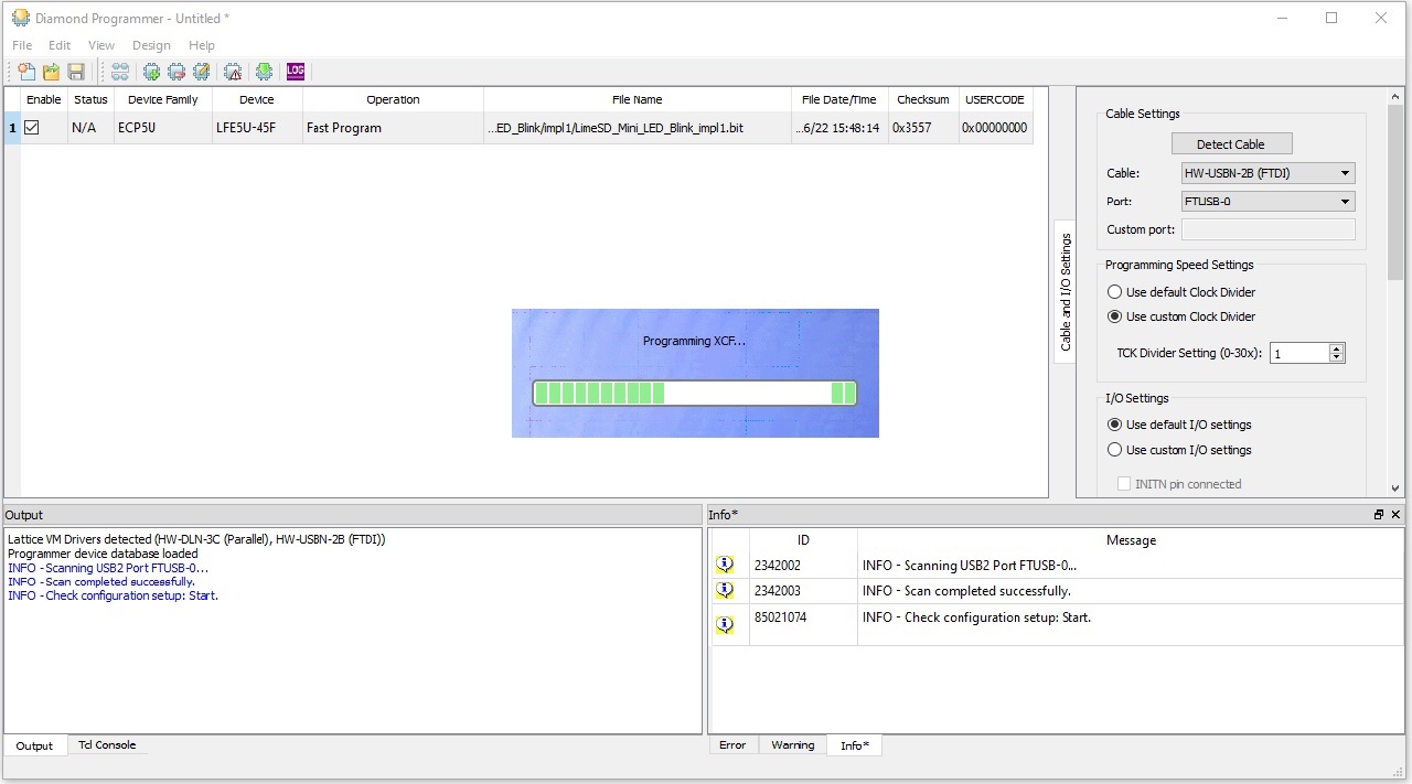
Figure 7: Programming procedure
After successful programming operation “Status” field will change to “PASS” highlihted in green as shown in Figure 8 and FPGA will start execution of a new gateware.
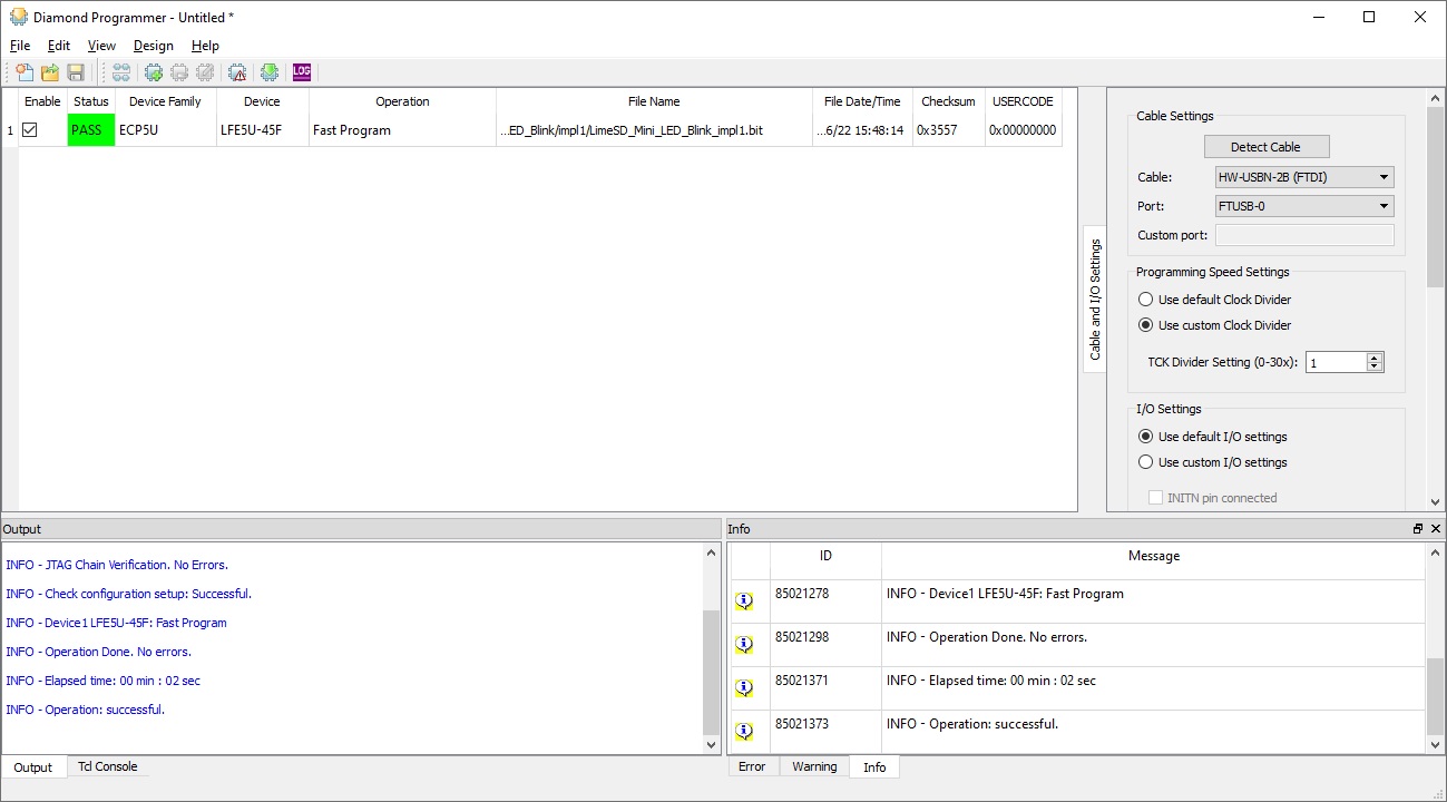
Figure 8: Successful programming result
Flash programming
IMPORTANT! Backgroud programming has to be enabled first by programming lms7_trx_preflash_gw.bit file with “RAM programing” procedure.
In context menu press “Edit -> Device properties” and in section “Device Operation” set “Access mode” to “SPI Flash Background Programming” and “Operation” to “SPI Flash Erase,Program,Verify”.
Load appropriate programming file (gateware, bitstream) and set the remaining parameters for Winbond W25Q128JV flash memory as shown in the image below and then press “OK”.
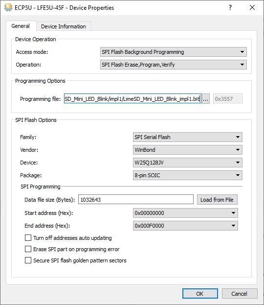
Figure 8: LimeSDR Mini v2 board and FT2232H Mini module connections
The main program window should look like shown in figure 9.
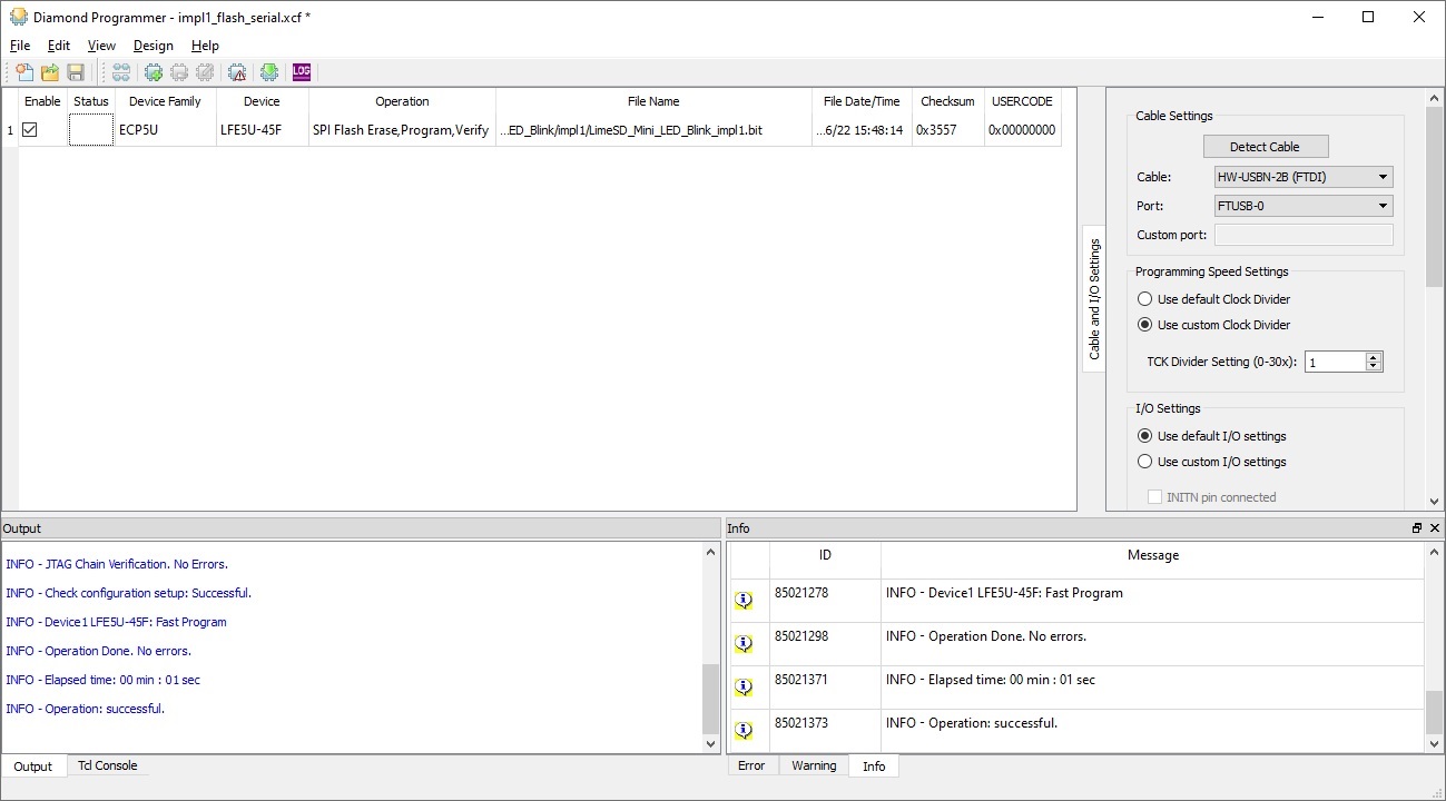
Figure 9: Main program window
In context menu press “Design -> Program” and Flash programming procedure will start, as shown in Figure 10.
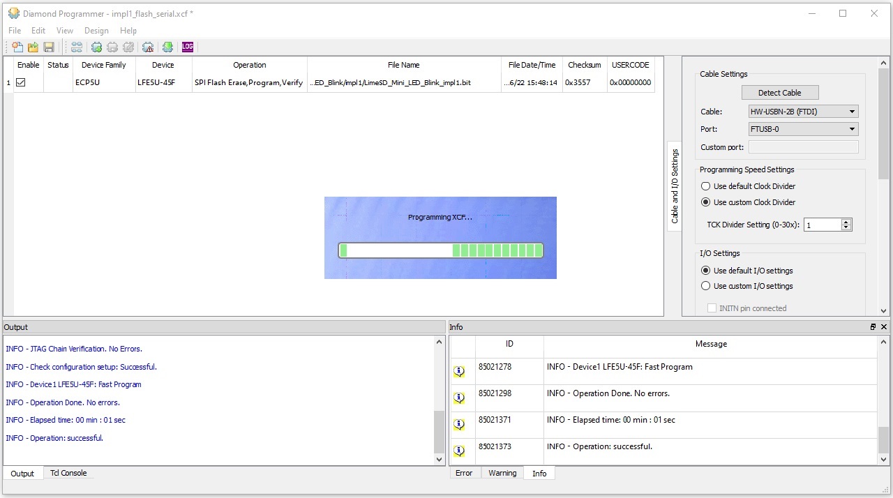
Figure 10: Flash in progress
After successful programming operation “Status” field will change to “PASS” highlihted in green as shown in Figure 11 and FPGA will start execution of a new gateware.
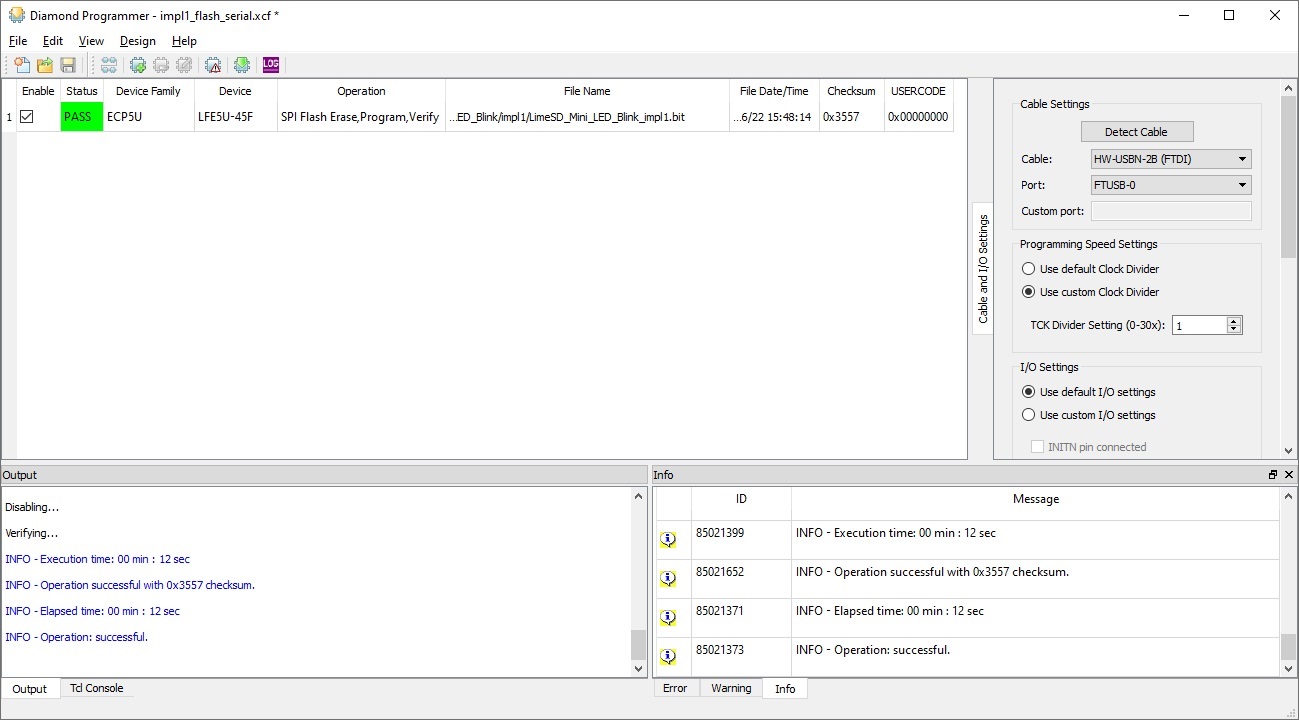
Figure 11: Successful programming
You can now save project for future use by selecting menu item “File -> Save”.
FPGA programming using Lattice Diamond software
Open .ldf project File->Open->Project…
FPGA SRAM programming
Open programmer setup file: ./LimeSDR-Mini_bitstreams/impl1_sram.xcf
Select .bit file : ./LimeSDR-Mini_bitstreams/lms7_trx_impl1.bit
Click Program.
You should see blinking LED1 in green colour.
FPGA FLASH programming
First program bitstream file to enable background programming:
Open programmer setup file: ./LimeSDR-Mini_bitstreams/impl1_sram.xcf
Select .bit file : ./LimeSDR-Mini_bitstreams/lms7_trx_preflash_gw.bit
Click Program
Program Flash:
Open programmer setup file: ./LimeSDR-Mini_bitstreams/impl1_flash_dualboot.xcf
Select .mcs file : ./LimeSDR-Mini_bitstreams/lms7_trx_impl1_dualboot.mcs
Click Program
You should see blinking LED after reapplying power to board